- 您现在的位置:买卖IC网 > Sheet目录1993 > DS1123LE-100+ (Maxim Integrated Products)IC DELAY LINE 256TAP 16-TSSOP
DS1123L
3.3V, 8-Bit, Programmable Timing Element
10
_____________________________________________________________________
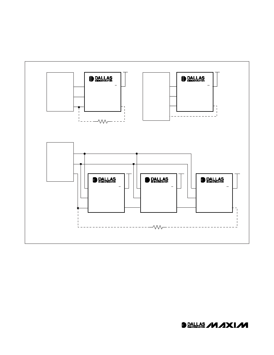
To read the current values stored by the 3-wire
device(s), the latch must be enabled and the value of Q
must be read and then written back to D before the
register is clocked. This causes the current value of the
register to be written back into the DS1123L as it is
being read. This can be accomplished in a couple of
different ways. If the microprocessor has an I/O pin that
is high impedance when set as an input, a feedback
resistor (generally between 1k
Ω and 10kΩ) can be
used to write the data on Q back to D as the value is
read (see Figure 5a). If the microprocessor has an
internal pullup on its I/O pins, or only offers separate
input and output pins, the value in the register can still
be read. The circuit shown in Figure 5b allows the Q
values to read by the microprocessor, which must write
the Q value to D before it can clock the bus to read the
next bit. If the Q values are read without writing them to
D (with the pullup or otherwise), the read is destructive.
A destructive read cycle likely results in an undesirable
change in the delay setting.
Figure 5c shows how to cascade multiple DS1123L’s
onto the same 3-wire bus. One important detail of writ-
ing software for cascaded 3-wire devices is that all the
devices on the bus must be written to or read from dur-
ing each read or write cycle. Attempting to write to only
the first device (U1) would cause the data stored in U1
MICROPROCESSOR
OUTPUT
I/O PIN
LE
CLK
DQ
RFB
MICROPROCESSOR
OUTPUT
INPUT
A) USING A FEEDBACK RESISTOR WITH AN I/O PIN FOR READING
THE DS1123L
B) USING A SEPARATE INPUT PIN TO READ THE DS1123L
MICROPROCESSOR
LE
CLK
DQ
LE
CLK
DQ
LE
CLK
DQ
OUTPUT
I/O PIN
RFB
C) CASCADING MULTIPLE DS1123L'S ON A 3-WIRE BUS
VCC
LE
CLK
DQ
P/S
DS1123L
U1
U2
U3
DS1123L
Figure 5. Using the Serial Interface
发布紧急采购,3分钟左右您将得到回复。
相关PDF资料
DS1124U-25+T
IC DELAY LINE 256TAP 10-USOP
DS1135LU-300/T&R
IC DELAY LINE 300NS 8-USOP
DS1135Z-12/T&R
IC DELAY LINE 12NS 8-SOIC
DS1181LE+
IC CLOCK MOD SS 8-TSSOP
DS1243Y-120
IC NVSRAM 64KBIT 120NS 28DIP
DS1244W-120IND
IC NVSRAM 256KBIT 120NS 28DIP
DS1248Y-70IND
IC NVSRAM 1MBIT 70NS 32DIP
DS1251WP-120+C02
IC NVSRAM 34PWRCP
相关代理商/技术参数
DS1123LE-200
功能描述:延迟线/计时元素 Programmable 3.3V 8 Bit Timing Element RoHS:否 制造商:Micrel 功能:Active Programmable Delay Line 传播延迟时间:1000 ps 工作温度范围: 封装 / 箱体:QFN-24 封装:Tube
DS1123LE-200+
功能描述:延迟线/计时元素 Programmable 3.3V 8 Bit Timing Element RoHS:否 制造商:Micrel 功能:Active Programmable Delay Line 传播延迟时间:1000 ps 工作温度范围: 封装 / 箱体:QFN-24 封装:Tube
DS1123LE-25
功能描述:延迟线/计时元素 Programmable 3.3V 8 Bit Timing Element RoHS:否 制造商:Micrel 功能:Active Programmable Delay Line 传播延迟时间:1000 ps 工作温度范围: 封装 / 箱体:QFN-24 封装:Tube
DS1123LE-25+
功能描述:延迟线/计时元素 Programmable 3.3V 8 Bit Timing Element RoHS:否 制造商:Micrel 功能:Active Programmable Delay Line 传播延迟时间:1000 ps 工作温度范围: 封装 / 箱体:QFN-24 封装:Tube
DS1123LE-50
功能描述:延迟线/计时元素 Programmable 3.3V 8 Bit Timing Element RoHS:否 制造商:Micrel 功能:Active Programmable Delay Line 传播延迟时间:1000 ps 工作温度范围: 封装 / 箱体:QFN-24 封装:Tube
DS1123LE-50+
功能描述:延迟线/计时元素 Programmable 3.3V 8 Bit Timing Element RoHS:否 制造商:Micrel 功能:Active Programmable Delay Line 传播延迟时间:1000 ps 工作温度范围: 封装 / 箱体:QFN-24 封装:Tube
DS1123LS-200
功能描述:延迟线/计时元素
RoHS:否 制造商:Micrel 功能:Active Programmable Delay Line 传播延迟时间:1000 ps 工作温度范围: 封装 / 箱体:QFN-24 封装:Tube
DS1123LS-25
功能描述:延迟线/计时元素
RoHS:否 制造商:Micrel 功能:Active Programmable Delay Line 传播延迟时间:1000 ps 工作温度范围: 封装 / 箱体:QFN-24 封装:Tube